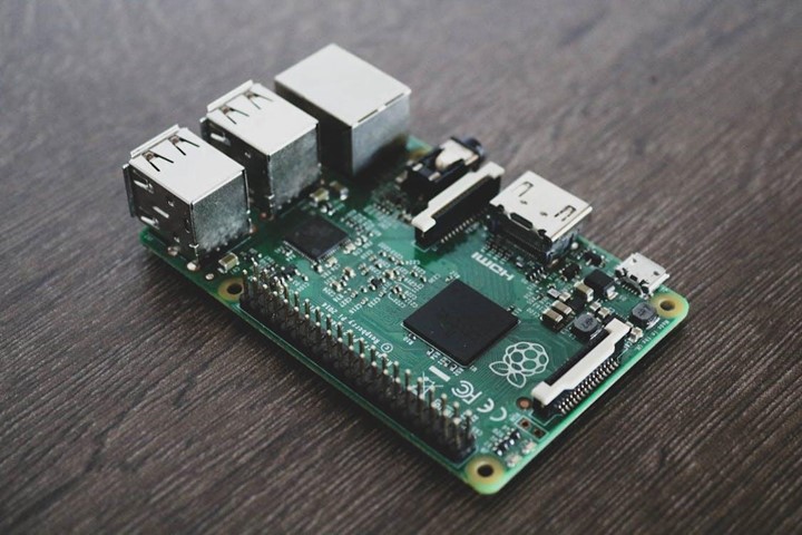
When you hear about electronic devices—whether it's your smartphone, laptop, or even the washing machine—you may not think about the small, green board that powers them all. Yet, this tiny piece of technology, known as a printed circuit board (PCB), is the backbone of modern electronics. In fact, the PCB market worldwide is expected to grow from $63.1 billion in 2021 to $72.3 billion by 2026.
This surge highlights how crucial PCBs are in today's tech-driven world. But the question is, what is PCB manufacturing exactly, and how does it work? Let's dive in and explore everything in detail.
When we talk about what is PCB in manufacturing, we're referring to the process of creating printed circuit boards that are used to mechanically support and electrically connect electronic components.
These boards serve as the foundation of virtually all electronic devices. The manufacturing process starts with a design—typically created using computer-aided design (CAD) software—that outlines where each component will be placed on the board and how the electrical connections will be made.
The design is then translated into a physical board through a series of steps, including etching, drilling, and plating. For example, in a simple single-layer PCB, a copper sheet is laminated onto a non-conductive substrate, and unwanted copper is etched away to leave behind the desired circuit pattern. On the other hand, in more complex multi-layer boards, multiple layers of circuits are stacked and connected through vias—which are basically small holes filled with conductive material.
When it comes to the types of PCBs, there are many—depending on the complexity and application. Firstly, there are single-sided boards with components on just one side, double-sided boards with components on both sides, and multi-layer boards that can have as many as 40 or more layers. Each type has its own set of challenges and requires different techniques to ensure quality and reliability.
So, when we ask what is PCB in manufacturing, we're talking about a specialized process that transforms a design into a circuit board that can withstand the demands of modern electronics.
Now, let's get into what material is flexible PCB manufacturing involves. For starters, the materials used in PCB manufacturing are carefully selected to ensure the circuit board can handle the electrical and mechanical stresses it will encounter. The base material, or substrate, is typically made from a fiberglass-reinforced epoxy resin, commonly known as FR4. This material provides the necessary strength and rigidity while being an excellent insulator to prevent unwanted electrical currents.
On top of the substrate, a thin layer of copper is applied, which will eventually form the conductive pathways of the PCB. Depending on the design, one or both sides of the board may be coated with copper. This copper layer is essential for creating the electrical connections between components and ensuring efficient functionality. The copper thickness can vary depending on the application's requirements, with thicker copper layers used in boards that need to handle higher currents.
In addition, other materials are used to protect and enhance the PCB's functionality. A solder mask is applied to the board to prevent solder from bridging between conductors and causing short circuits. This is the green (or sometimes other colored) layer you see on most PCBs. There's also a silkscreen layer, which is used to add labels and markings to the board for easier assembly and troubleshooting.
So, if you ask, what material is PCB manufacturing? Simply put, it's a combination of fiberglass, epoxy, copper, solder mask, and silkscreen, each playing a critical role in the board's performance.
Before a PCB can be manufactured, certain files are required to guide the process. These files are like the blueprint for the board, detailing everything from the layout of the components to the exact dimensions of the holes that need to be drilled. So, what files are required for PCB manufacturing?
The most important file is the Gerber file, which contains the information needed to create the different layers of the PCB. Each layer of the board—whether it's the copper layer, solder mask, or silkscreen—has its own Gerber file. These files are essential and used by the manufacturing equipment to accurately etch, drill, and print the PCB, ensuring precision in the final assembly.
In addition to Gerber files, an Excellon drill file is needed. This file provides the exact locations and sizes of all the holes that need to be drilled into the board. These holes can be used for mounting components, connecting different layers of the board, or attaching the board to a case or chassis.
Another critical file is the Bill of Materials (BOM), which lists all the components that will be placed on the board. The BOM includes information like part numbers, quantities, and descriptions, ensuring that the correct components are used during assembly for error-free production.
Finally, an assembly drawing file is often provided, showing where each component should be placed on the board. Together, these files—Gerber, Excellon, BOM, and assembly drawing—are essential for guiding the manufacturing and ensuring the final product meets design specifications.
In wrapping up our exploration of PCB manufacturing, it's clear that this process is much more than just assembling components on a board. It's about crafting the very heart of our modern electronic devices with precision and foresight. From the initial design stages using Computer-Aided Design (CAD) software to the layering and drilling guided by some of the most critical files like Gerber and Excellon, every step is pivotal in shaping the functionality and reliability of the final product.
The choice of materials—from the robust FR4 substrate to the conductive copper layers and protective solder mask—ensures that each PCB can stand up to the demands of its environment, whether it's in a consumer gadget or an industrial machine. The meticulous attention to detail required in PCB manufacturing underscores its importance in the broader electronics industry.
As technology continues to advance at a breakneck pace, the role of sophisticated, well-manufactured PCBs will only grow more critical. So, next time you power up your device, remember the intricate process of PCB manufacturing that made it all possible. It's a world where design meets functionality, creating the unseen yet essential platforms that keep our modern, digital lives running smoothly.


